Project TELEGRAPH (Part 3): Bare Metal, Bit-Banging, and the 4MB Heist
Overview
I expected to just load up an Arduino "Blink" sketch and start mapping pins. The toolchain had other plans.
1. Bootstrapping the Bare Metal (The PlatformIO Struggle)
The STM32F105 "Connectivity Line" is the weird middle child of the ST lineup, less powerful than the F107-line, more like F103, but with full USB controller (with host mode). It was used for downloading data from the USB drive - neat, could be useful. When I've tried to compile a basic PlatformIO project, I hit a wall: the F105RB is actually mocked in standard PlatformIO Arduino definitions. It lacks linker script, proper board definition and some other things. This is probably due to the fact, that there is no popular development board with F105, as far as I know...
To get code to compile, I created a custom board manifest (genericSTM32F105RB.json) and copied the linker script from some other board with F103 chip - those should be almost the same due to similarities between memory layouts for those chip families.
But compiling is only half the battle. When I flashed the firmware, I got just a brick The MCU did absolutely nothing. No UART output, no GPIO toggling.
The culprit? The clock. It seems the initialization for the F105 is totally missing.
To fix this, I had to bypass the framework's initialization and write a custom SystemClock_Config. I manually forced
the microcontroller to use its High-Speed Internal (HSI) oscillator and configured the Phase-Locked Loop (PLL) to hit
our target frequency. This is the snippet of the clock init:
 1// Bypassing the Arduino core to force the internal oscillator
 2extern "C" void SystemClock_Config(void) {
 3  RCC_OscInitTypeDef RCC_OscInitStruct = {0};
 4  RCC_ClkInitTypeDef RCC_ClkInitStruct = {0};
 5
 6  // 1. Setup HSI and Main PLL
 7  RCC_OscInitStruct.OscillatorType = RCC_OSCILLATORTYPE_HSI;
 8  RCC_OscInitStruct.HSIState = RCC_HSI_ON;
 9  RCC_OscInitStruct.HSICalibrationValue = RCC_HSICALIBRATION_DEFAULT;
10
11  // On F105, HSI is always divided by 2 before reaching the PLL
12  // 8MHz / 2 = 4MHz.
13  // 4MHz * 9 = 36MHz (Let's start safe at 36MHz)
14  RCC_OscInitStruct.PLL.PLLState = RCC_PLL_ON;
15  RCC_OscInitStruct.PLL.PLLSource = RCC_PLLSOURCE_HSI_DIV2;
16  RCC_OscInitStruct.PLL.PLLMUL = RCC_PLL_MUL9;
17
18  if (HAL_RCC_OscConfig(&RCC_OscInitStruct) != HAL_OK) {
19    while(1); // Hang here if config fails
20  }
21
22  // 2. Configure Clock Tree
23  RCC_ClkInitStruct.ClockType = RCC_CLOCKTYPE_HCLK|RCC_CLOCKTYPE_SYSCLK
24                              |RCC_CLOCKTYPE_PCLK1|RCC_CLOCKTYPE_PCLK2;
25  RCC_ClkInitStruct.SYSCLKSource = RCC_SYSCLKSOURCE_PLLCLK;
26  RCC_ClkInitStruct.AHBCLKDivider = RCC_SYSCLK_DIV1;
27  RCC_ClkInitStruct.APB1CLKDivider = RCC_HCLK_DIV2; // APB1 must be <= 36MHz
28  RCC_ClkInitStruct.APB2CLKDivider = RCC_HCLK_DIV1;
29
30  if (HAL_RCC_ClockConfig(&RCC_ClkInitStruct, FLASH_LATENCY_1) != HAL_OK) {
31    while(1);
32  }
33}
It's from this file in the project.
Suddenly, the chip woke up.
2. "Ping..." (Bridging the Gap)
With the clock tree stable, I routed the UART output through the ESP32 wireless serial bridge (ser2net) we built in
the last post.
When I've opened a TCP socket to the ESP32 on my laptop
Ping... was popping up
on my terminal. The chip's heart was beating. We had full, untethered code execution and debugging across the room.
Additionally I was changing the state on PC6 pin, since it was one of those I had available on some connector and I
could check that it's state was changing using the multimeter (if UART would've not worked).
3. Cracking the Matrix (The Display Drivers)
Now for the fun part: making it glow. Board consists of basically 3 displays:
- the 7-segment (12 digits) LED display driven by TM1629A chip,
- 21x14 green led matrix driven by 3 SM16126D shift registers,
- 70x14 red led matrix driven by 6 SM16126D shift registers,
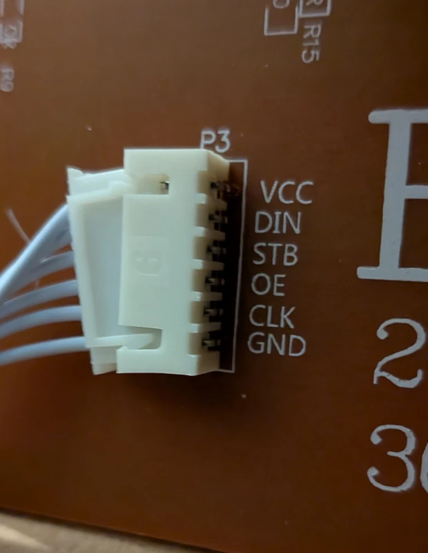
Connections to the matrices are well described:
The TM1629A (The 7-Segment Driver)
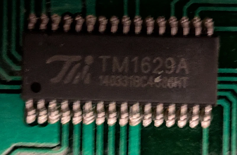
Tracing the traces from the 7-segment displays led me to a TM1629A. This is a dedicated LED drive control IC that handles its own internal multiplexing. It doesn't need constant babying from the CPU; you just send it a serial command containing the digits you want to display, and it latches them onto the 7-segment screen. First I had to check for the 3 signals used by this chip (strobe, clock and data in/out). I've used multimeter in continuity test mode and I've identified fo9llowing connections leading to my MCU:
| Function | TM's Pin | MCU |
|---|---|---|
| DIO | 7 | PB4 |
| CLK | 8 | PB3 |
| STB | 9 | PB5 |
Next I had to identify the addressing. It was interesting, since TM1629A supports 16 digits with 8 segments (7 segments + dot), the connection wasn't straightforward. I've written this scanner to identify proper addressing. It led me to implement this driver.
The most interesting part is this function:
 1// Converts digitIdx to actual address used by TM1629
 2// NOTE: 10, 11 are not used (there is hole in addressing)
 3const uint8_t digitToBit[] = {0, 1, 2, 3, 4, 5, 6, 7, 8, 9, 12, 13};
 4
 5/* for segData, bit means which segment from A-G is lit, e.g:
 6               pGFEDCBA
 7   0 → 0x3F (0b00111111)
 8   1 → 0x06 (0b00000110)
 9   2 → 0x5B (0b01011011)
10   3→  0x4F (0b01001111)
11
12      -A-
13     |   |
14     F   B
15     |   |
16     +-G-+
17     |   |
18     E   C
19     |   |
20      -B-  p
21
22NOTE: dp (decimal point) is not used, we don't have any decimal points on our display
23*/
24void tm_setDigitRaw(uint8_t digitIdx, uint8_t segData) {
25  if (digitIdx > 11) return;
26
27  uint8_t bitIdx = digitToBit[digitIdx];
28  uint8_t byteOffset = (bitIdx >= 8) ? 1 : 0;
29  uint8_t bitMask = 1 << (bitIdx % 8);
30
31  // Loop through segments A(0) to G(6)
32  for (uint8_t seg = 0; seg < 7; seg++) {
33    // TM1629A Addresses: A=0x00, B=0x02, C=0x04, D=0x06, E=0x08, F=0x0A, G=0x0C
34    uint8_t addr = (seg * 2) + byteOffset;
35
36    if (segData & (1 << seg)) {
37      tm_framebuffer[addr] |= bitMask;  // Turn ON segment
38    } else {
39      tm_framebuffer[addr] &= ~bitMask; // Turn OFF segment
40    }
41  }
42
43  // `tm_framebuffer` is written to chip's registers during `tm_updateDisplay` call
44}
The SM16126D (The LED Matrix)
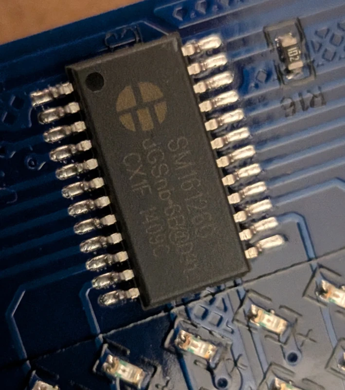
The main dot-matrix display was a completely different beast. Tracing these lines led to a bank of SM16126D ICs. These are effectively high-power shift registers. Unlike the TM1629A, these chips have no memory and no internal multiplexer. It seems, that first of the SM16126D's was controlling rows and rest of them were responsible for their set of columns.
Using multimeter, I've identified the connections:
| P3 Pin | MCU | First SM16126D Pin |
|---|---|---|
| CLK | PB12 | 3 |
| OE | PB13 | 21 |
| STB | PB14 | 4 |
| DIN | PA13 | 2 |
| DIN (big screen) | PB15 | 2 |
To light up the matrix, I had to do the heavy lifting in software. I wrote a custom C++ multiplexing loop to push raw framebuffers into the shift registers. Because the SM16126D's forget their state the moment you move to the next row, this code had to be fast.
We now had complete programmatic control over both the 7-segment readout and the raw LED matrix, all driven from our custom bare-metal firmware.
4. The Mystery 5-Pin Device (The Black Blob)
While tracing the board, I found an unknown 5-pin connector and cable leading to some glued device. The pins mapped to PC6, PC7, a 3.3V line, Ground, and a trace leading directly to a CR2032 coin cell battery.
The battery pin was the smoking gun: this was a Real-Time Clock (RTC).
I assumed it was I2C. However, here is the classic STM32 hardware trap: on the F105, PC6 and PC7 do not have hardware I2C support mapped to them. The original engineers just picked two random GPIOs to save board routing space.
Since I couldn't use the hardware Wire library (it would freeze looking for non-existent peripherals), I wrote a custom,
auto-detecting "Bit-Bang" I2C scanner. It manually
toggled the GPIOs HIGH and LOW to simulate the open-drain I2C protocol. It swept the bus and got an ACK on address
0x68.
It was a Maxim DS3231 RTC with temperature sensor. A quick read confirmed it: it spit out the factory epoch time (2000-01-01 04:48:51) and the live ambient temperature of my office (23.0°C).
5. Engaging the Final Boss (The Winbond SPI Flash)
The last major component was a 4MB (32Mbit) Winbond 25Q32FVS1G memory chip. I traced it back to the STM32's Hardware
SPI1 pins (PA4, PA5, PA6, PA7).
I wrote a quick reconnaissance scanner to ping
the chip's "Driver's License" (the JEDEC ID). It responded with EF 40 16 — loud and clear. I dumped first page and
spotted interesting stuff that looked like some numbers. First one (0x4c) looks like the length of this header (not
including this field). Rest probably is some project configuration.
10x00: 4C 00 00 00 01 40 58 00 10 00 00 0C 00 00 00 FF
20x10: 00 00 00 00 00 01 00 00 01 1C 00 00 00 00 00 00
30x20: 00 00 00 00 00 00 00 00 00 50 00 10 00 00 00 30
40x30: 00 00 00 FF 00 00 00 00 00 08 00 00 44 01 00 00
50x40: 00 00 00 00 00 00 00 00 00 00 00 00 00 FF FF FF
60x50: FF FF FF FF FF FF FF FF FF FF FF FF FF FF FF FF
7...
This chip holds the original configs and data for the proprietary Chinese software. It would be nice to take a look.
6. The 4MB Heist (Extracting the Brains)
Dumping 4 MBs of binary data over a 115200 baud UART connection, which is then piped through an ESP32 TCP network bridge, could be a recipe for disaster.
When I tried a simple Serial.write streaming loop, the network buffers overran, connection latency spiked, and bits dropped everywhere.
To reliably extract the data, I had to architect a custom Stop-and-Wait chunked protocol with built-in retry capability:
- The STM32 (arduino): Read a 4096-byte (4KB) chunk from the flash, calculate a strict CRC16-CCITT checksum, and send the 4098 bytes over the network.
- The Laptop (Python): Catch the chunk and run the exact same math. If the CRCs match, send an ACK. If the network corrupted a bit, send a NACK to force the STM32 to re-transmit that specific chunk.
 1# self-healing/retry logic
 2
 3while not block_accepted:
 4	# We expect exactly BLOCK_SIZE bytes of data + 2 bytes of CRC
 5	raw_chunk = ser.read(BLOCK_SIZE + 2)
 6
 7	if len(raw_chunk) != (BLOCK_SIZE + 2):
 8		print(f"\n[!] Network timeout or byte drop on Block {block}. Sending NACK...")
 9		ser.reset_input_buffer()
10		ser.write(b"NACK\n")
11		retries += 1
12		continue
13
14	data = raw_chunk[:BLOCK_SIZE]
15	received_crc = (raw_chunk[BLOCK_SIZE] << 8) | raw_chunk[BLOCK_SIZE + 1]
16
17	calculated_crc = calculate_crc16(data)
18
19	if received_crc == calculated_crc:
20		ser.write(b"ACK\n")
21		dump_data.extend(data)
22		block_accepted = True
23	else:
24		print(f"\n[!] CRC Mismatch on Block {block} (Got {hex(received_crc)}, Expected {hex(calculated_crc)}). Sending NACK...")
25		ser.reset_input_buffer()
26		ser.write(b"NACK\n")
27		retries += 1
After several minutes of blinking lights and a few successfully caught network drops, the script finished. I ran a full-file CRC32 check against the physical chip. It was a flawless 1:1 hardware clone.
7. Unmasking the Ghost in the Machine (Data Forensics)
Time to see what we stole. I ran a hexdump on the extracted .bin file.
Glancing over the dump, I landed at address 0x00005000. Right away, I found an ASCII manifest referencing yxled.prj,
yxled.dat, and autime.cfg. It looked exactly like files that were written to the USB drive used for programming the
display, so they're just copied to embedded flash.
 1❯ hexdump -C -s 0x5000 hazk03_flash_spi_dump.bin -n 0xea
 200005000  e8 00 00 00 79 78 6c 65  64 2e 70 72 6a 7c 32 30  |....yxled.prj|20|
 300005010  32 34 2d 30 37 2d 32 36  20 30 38 3a 34 39 3a 35  |24-07-26 08:49:5|
 400005020  39 7c 37 36 7c 41 34 44  43 32 44 2d 34 41 35 38  |9|76|A4DC2D-4A58|
 500005030  42 35 35 36 2d 32 46 41  34 44 42 0d 0a 79 78 6c  |B556-2FA4DB..yxl|
 600005040  65 64 2e 64 61 74 7c 32  30 32 34 2d 30 37 2d 32  |ed.dat|2024-07-2|
 700005050  36 20 30 38 3a 34 39 3a  35 39 7c 33 32 34 7c 31  |6 08:49:59|324|1|
 800005060  38 43 30 36 35 2d 38 37  38 43 32 45 46 44 2d 32  |8C065-878C2EFD-2|
 900005070  33 31 38 42 33 0d 0a 61  75 74 69 6d 65 2e 63 66  |318B3..autime.cf|
1000005080  67 7c 32 30 31 36 2d 30  36 2d 32 39 20 31 30 3a  |g|2016-06-29 10:|
1100005090  35 31 3a 30 30 7c 34 33  7c 30 30 30 30 30 30 2d  |51:00|43|000000-|
12000050a0  30 30 30 30 30 30 30 30  2d 30 30 30 30 30 30 0d  |00000000-000000.|
13000050b0  0a 61 75 6c 69 67 68 74  2e 63 66 67 7c 32 30 31  |.aulight.cfg|201|
14000050c0  31 2d 30 38 2d 30 32 20  31 33 3a 30 33 3a 33 34  |1-08-02 13:03:34|
15000050d0  7c 34 35 7c 34 38 34 38  34 39 2d 33 36 33 36 33  ||45|484849-36363|
16000050e0  36 33 37 2d 34 38 34 38  34 38                    |637-484848|
17000050e8
The manifest showed the exact date the board was last flashed (2024-07-26 08:49:59). It also explicitly stated the size
of the compiled graphics payload (yxled.dat): 324 bytes. There are also some UID's, probably acting as file checksums
(e.g. A4DC2D-4A58B556-2FA4DB). Interesting... It looks like files themselves are located at (looking at full dump and
len fields - comparing them to the sizes in this manifest):
- 0x0 (
yxled.prj, len byte=76) - this would contain project configuration details, like width, height, animations, etc. - 0x3000 (
autime.cfg, which has len byte=43 and uid for this file is all zeros, because content at this offset is all zeros - confirms theory about this being checksum) - clock settings?, - 0x4000 (
aulight.cfg, len byte=45) - no idea, - 0x6000 (
yxled.dat, len bytes=324) - actual graphic to be displayed.
But what about the graphics themselves? Let's take a look at the yxled.dat (0x6000) dump, skipping len bytes:
 1❯ hexdump  hazk03_flash_spi_dump.bin -s 0x6004 -n 0x144 -v
 20006004 0050 0010 0000 0000 0000 0000 0000 0000
 30006014 0000 0000 0000 0000 0000 0000 0000 0000
 40006024 0000 0000 0000 0000 0000 0000 0000 0000
 50006034 0000 0000 c003 0000 0000 0000 0000 0000
 60006044 0000 0000 0000 0000 c003 0000 0000 0000
 70006054 0000 0000 0000 0000 0000 0000 c003 0000
 80006064 0000 0000 0000 0000 0000 0000 0000 ff01
 90006074 ffc3 ffc1 00c0 0000 0000 0000 0000 0000
100006084 0000 e303 f3e3 f7f3 00e0 0000 0000 0000
110006094 0000 0000 0000 0100 c0f3 c0f7 0000 0000
1200060a4 0000 0000 0000 0000 0000 ff03 c0f3 80ff
1300060b4 0000 0000 0000 0000 0000 0000 0000 e107
1400060c4 c0f3 80ff 0000 0000 0000 0000 0000 0000
1500060d4 0000 8307 c0f3 c0f7 0000 0000 0000 0000
1600060e4 0000 0000 0000 cf07 f3f3 f7f3 00e0 0000
1700060f4 0000 0000 0000 0000 0000 ff03 ffff ffc1
180006104 00c0 0000 0000 0000 0000 0000 0000 0000
190006114 0000 0000 0000 0000 0000 0000 0000 0000
200006124 0000 0000 0000 0000 0000 0000 0000 0000
210006134 0000 0000 0000 0000 0000 0000 0000 0000
220006144 0000 0000
By analyzing the data, we can see the image is exactly 80 pixels wide and 16 pixels high. The first 4 bytes
(0050 0010) act as the header (which likely translates to a width of 80 16-bit words/160 bits, and a height of 16),
leaving exactly 320 bytes of payload. At 1 bit-per-pixel, 320 bytes perfectly fills a 160x16 grid.
After parsing the bytes in Big-Endian bit order, we have the graphic that was programmed using the manufacturers software. Nice.
 1................................................................................
 2................................................................................
 3...................................**...........................................
 4...................................**...........................................
 5...................................**...........................................
 6...........................******..******..******...............................
 7...........................***.***.***.***.*******..............................
 8...............................***.**...*****...................................
 9...........................*******.**...*****...................................
10..........................****.***.**...*****...................................
11..........................***..***.**...*****...................................
12..........................***.****.***.***.*******..............................
13...........................**************..******...............................
14................................................................................
15................................................................................
16................................................................................
8. Conclusion & Next Steps: Graduating from Arduino
We mapped the hardware, dumped the flash, and built a custom display multiplexer. But there is a glaring architectural problem moving forward.
The Arduino's loop() architecture is fundamentally single-threaded and blocking. If I want to add a USB Host
functionality (use the actual cool stuff the connectivity-line offers) and bridge it to esp32 (like for example adding
usb-rs485 adapter), the display multiplexing will stutter every time the USB stack triggers an interrupt.
In the next phase, we are ditching the Arduino framework entirely and going for some nice RTOS.
Posts in this series
- Project TELEGRAPH (Part 1): Rescuing a $15 LED Matrix from Software Purgatory
- Project TELEGRAPH (Part 2): Escaping the Cables with a Custom ESP32 Wireless Flasher
- Project TELEGRAPH (Part 3): Bare Metal, Bit-Banging, and the 4MB Heist